Semicon 2.0: India's support for chip fabs, packaging and design
Semicon 2.0 is the scheme for India's chip industry from MeitY, the Ministry of Electronics and Information Technology, notified on August 31, 2026. It pays 40% of eligible capital cost for a large silicon wafer fab and 25% to 35% for other fabs and packaging units. Applications are first open for three years, through the India Semiconductor Mission's portal.
Published and updated
What is Semicon 2.0?
Semicon 2.0 is MeitY's scheme of fiscal support for chip design and manufacturing, following the first Semicon India program. The Cabinet approved it on July 15, 2026 with an outlay of ₹1.27 lakh crore, the government told the Lok Sabha on August 5, 2026. MeitY notified it on August 31, 2026, in six pillars.
- Chip design: strategic and commercial chips, and an incentive on new chips' sales (Semicon 2.0 notification, opens in a new tab, paras 3.1 to 3.3).
- Machines and materials: equipment, materials and test facilities (para 3.4).
- More fabs: silicon, compound, photonics, sensor, discrete and display fabs (paras 3.5 to 3.7).
- Packaging: assembly, testing, marking and packaging (ATMP) and outsourced semiconductor assembly and test (OSAT) units (para 3.8).
- R&D: up to 75% of project cost, state incentives included (para 3.9).
- Talent: the same, for Indian academic and R&D institutions, scientific societies and training institutions (para 3.10).
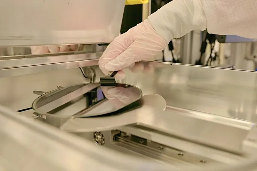
The India Semiconductor Mission (ISM), a business division of the Digital India Corporation, runs the scheme as its nodal agency (notification, opens in a new tab, para 6.1; guidelines, opens in a new tab, para 2.19). It sits with MeitY's other electronics schemes in our MeitY guide.
MeitY's guidelines of September 16, 2026, opens in a new tab cover pillars 2 to 4; our insight on those guidelines reads them step by step.
How much support does each kind of plant get?
Semicon 2.0 pays a share of eligible capital cost: 40% for a large silicon wafer fab, 35% for compound semiconductor, photonics, sensor, discrete and display fabs and for advanced packaging, 25% for legacy packaging, and 30% for equipment, materials and test units. Each must clear a minimum capacity, investment and revenue.
| Plant | Support | Minimum | Source |
|---|---|---|---|
| Silicon wafer fab, 300 mm | 40% of eligible capital cost | 40,000 wafer starts a month; ₹20,000 crore invested; ₹7,500 crore revenue | Para 3.5.3 |
| Compound semiconductor, photonics, sensor (MEMS) or discrete fab | 35% of eligible capital cost | 150 mm wafers or more (200 mm for sensors, 100 mm for photonics); 500 wafer starts a month; ₹500 crore invested; ₹200 crore revenue | Para 3.6.3 |
| OLED (Generation 6 or above) or LCD (Generation 8 or above) display fab | 35% of eligible capital cost | 30,000 OLED or 60,000 LCD panels a month; ₹10,000 crore invested; ₹5,000 crore revenue | Para 3.7.3 |
| Micro LED display fab | 35% of eligible capital cost | 500 square meters of panels a month; ₹1,500 crore invested; ₹600 crore revenue | Para 3.7.3 |
| Advanced packaging and advanced substrates | 35% of eligible capital cost | ₹1,000 crore invested; ₹200 crore revenue | Para 3.8.3 |
| Legacy packaging | 25% of eligible capital cost | ₹1,000 crore invested; ₹200 crore revenue | Para 3.8.3 |
| Equipment, sub-assemblies and components | 30% of capital cost, plus a production-linked incentive of 10% falling to 2% of the value of parts sourced from makers in India, for five years from fiscal 2028-29, capped overall at 50% of eligible capital cost | ₹300 crore invested; ₹120 crore revenue | Para 3.4.3(d) |
| Equipment R&D facility | 30% of capital cost | ₹300 crore invested; ₹120 crore revenue | Para 3.4.3(a) |
| Semiconductor-grade materials | 30% of capital cost | ₹50 crore invested; ₹20 crore revenue | Para 3.4.3(b) |
| Test and characterization facility | 30% of capital cost | ₹100 crore invested; ₹40 crore revenue | Para 3.4.3(c) |
Pari-passu means ISM pays its share pro rata, once the company's matching share is in a no-lien account (guidelines, opens in a new tab, para 2.20). Land, temporary structures, technology transfer, interest during construction and R&D don't count as eligible capital cost (para 4.1).
Fab and packaging applicants must own or possess production-grade licensed technology, already demonstrated and available for commercial production (notification, opens in a new tab, paras 3.5.3 to 3.8.3; guidelines para 2.21).
The fab rate isn't 50%
Some pages still say Semicon 2.0 pays 50% for fabs. It pays 40% for silicon wafer fabs and 35% for other fabs (notification paras 3.5.3 to 3.7.3).
Who can claim the chip design support?
Semicon 2.0's chip design support goes to companies incorporated and headquartered in India, with a significant operational and manpower presence there, and owned and controlled by Indian citizens. For commercial chips, companies owned and controlled by Overseas Citizens of India also qualify. Indian academic institutions can also use the national design tools grid and wafer runs.
- Strategic chips: C-DAC issues requests for proposals, picks by competitive bidding and co-owns the IP (Semicon 2.0 notification, opens in a new tab, paras 3.1.4 and 3.1.5).
- Commercial chips: design (EDA) tools and multi-project wafer runs for Indian academic institutions, startups and MSMEs, and IP cores and post-silicon validation for every eligible company. The IP and design files stay in India (paras 3.2.4 and 3.2.5).
- Product Design Linked Incentive: seed funding of 50% of project cost or ₹15 crore, whichever is lower, for startups and MSMEs; royalty financing for other eligible companies; and equity co-investment beside venture capital or private equity investors (para 3.2.5).
- Deployment-linked incentive: 9% of net sales of newly launched chips for five years, up to ₹30 crore per application and ₹120 crore per company (para 3.3.4).
How do you apply for Semicon 2.0?
You apply for Semicon 2.0 online on the India Semiconductor Mission's portal, in a window first open for three years. For the machines and materials, fab and packaging pillars, the window runs from MeitY's guidelines of September 16, 2026, the fee is ₹10 lakh plus GST and isn't refunded, and the Union Cabinet approves each project.
1. Register on ISM's portal
Apply online, in the Annexure-1 format (guidelines, opens in a new tab, paras 7.1 and 7.2).
2. Set up an Indian project company
Support goes only to a Project Company incorporated in India for the scheme, at least 51% held by the applicant, its promoter or group (paras 3.1 and 13.13; Annexure-1).
3. File the report and the fee
Send the detailed project report and proof of the ₹10 lakh plus GST fee (Annexure-1). The integrity undertaking asks you to disclose agents and payments to intermediaries (Annexure-4).
4. Wait for the acknowledgment
ISM acknowledges the application, preferably within 45 days. That isn't approval, and spending before it isn't reimbursed (paras 3.5 and 7.3).
5. Go through appraisal and the Cabinet
ISM appraises the technology and finances, preferably within six months of acknowledging, and MeitY puts its recommended projects to the Union Cabinet for approval (paras 8.1 to 8.4; notification para 7.4). These are ISM's targets, not approval times.
6. Sign and claim
Sign the Fiscal Support Agreement, open a no-lien bank account and claim as needed. The unit must then keep producing for at least three years after the whole project starts commercial production (paras 9.1, 9.2, 10.1 and 13.4).
The MeitY Secretary approves design and talent projects below ₹100 crore, the Minister up to ₹500 crore and the Cabinet above that (notification para 7.3).
What happened under the first program?
Under the first Semicon India program, launched in January 2022, the government approved 12 manufacturing projects in six states, with about ₹1.64 lakh crore of investment committed. Three plants had started commercial production. These are the government's own figures, given to the Lok Sabha on August 5, 2026.
The answer, opens in a new tab describes that program as support for fabs, display fabs, packaging and Indian-designed chips. On September 21, 2026, MeitY let the Minister extend the tenure, support period included, of projects under the modified program for compound, silicon photonics, sensor and discrete fabs and packaging units (addendum, opens in a new tab, para 7.7). Semicon 2.0's guidelines, opens in a new tab give the same power (para 8.5).
How IndusDesk helps with Semicon 2.0
We watch the authorities, tell you what each change means for your products and plans, represent you while a decision is still open, and carry the work through, with every step on record in your workspace.
Frequently asked questions
Which semiconductor projects has India approved?
Under the first Semicon India program, the government approved 12 manufacturing projects in Andhra Pradesh, Assam, Gujarat, Punjab, Odisha and Uttar Pradesh, with about ₹1.64 lakh crore committed. Three had started commercial production. That's from the government's answer to the Lok Sabha of August 5, 2026, opens in a new tab, which gives counts and states but no project names.
Can a foreign company claim MeitY's incentives directly, or must it set up in India?
Semicon 2.0's fab, packaging and machines and materials support goes only to a Project Company incorporated in India, at least 51% held by the applicant, its promoter or group (guidelines, opens in a new tab, paras 3.1 and 13.13; Annexure-1). A foreign company can take part in chip design only as a consortium partner of an eligible Indian company (notification, opens in a new tab, paras 3.1.3 and 3.2.3). Other schemes are in our guide to India's digital laws for foreign companies.
What does ECMS cover, and can you still apply?
The Electronics Component Manufacturing Scheme, opens in a new tab covers display and camera modules, passive and electro-mechanical components, PCBs, lithium-ion cells for digital devices, enclosures, their supply chain and capital equipment, plus optical transceivers since July 7, 2025, opens in a new tab. Segments A, B, C and E (modules, components and optical transceivers) closed on September 30, 2025, opens in a new tab, while segment D, supply chain and capital equipment, stays open until April 30, 2027 (ECMS portal, opens in a new tab). Our electronics manufacturing schemes guide has the rest.
Sources
- F. No. W-38/6/2025-IPHW, August 31, 2026 (CG-DL-E-31082026-275860): Semicon 2.0, Scheme for development of Semiconductor Design and Manufacturing Ecosystem in India, paras 3 to 7, opens in a new tab
- W-38/6/2025-IPHW, September 16, 2026: Guidelines for implementing the Machines and Materials, Fabs, and ATMP/OSAT pillars under Semicon 2.0, paras 2 to 13 and Annexures 1 and 4, opens in a new tab (PDF, 389 KB)
- W-38/21/2022-IPHW, September 21, 2026: Addendum to the guidelines of the modified program for compound semiconductor, silicon photonics, sensor and discrete fabs and ATMP/OSAT facilities, para 7.7, opens in a new tab
- Lok Sabha Starred Question No. 246, answered August 5, 2026: Promotion of semiconductor manufacturing and strengthening of electronics ecosystem, statement, opens in a new tab
- F. No. W/49/2024-IPHW, April 8, 2025: Electronics Component Manufacturing Scheme, para 4, opens in a new tab
- File No. W/49/2024-IPHW, July 7, 2025: Addendum-1 to the ECMS notification (optical transceivers), opens in a new tab
- File No. W/49/2024-IPHW, July 30, 2025: Amendment-2, extension of the ECMS application window, para 1, opens in a new tab
- ECMS portal, read October 31, 2026: notice 2 on the application windows, opens in a new tab